Development of the CVK Series S Type Driver
Recently, there has been an increasing demand to make equipment both higher-functioning and smaller. The CVK series S type driver is a product that was developed for customers who use stepper motors with self-built control boards. It has inherited the characteristics of the original CVK series of drivers and can be mounted onto boards, contributing to both smaller and higher performance equipment.
The changes from the original CVK series of drivers and the background of the development are explained in this article. More specifically, details regarding the circuit configuration adapted from the CVK series and the newly added functions (I/O, motor model number setting, SPI(Note 1) communication) are introduced here.
1. Introduction
Stepper motors are used in a broad variety of equipment, such as for semiconductor manufacturing, measurement, and analysis. In the realm of mass production of equipment that must be small, they are particularly useful with self-built control boards that have a programmable controller and a driver mounted on the same board.
Many self-built control boards employ a driver IC for commercial stepper motors. However, as equipment performance and noise requirements increase, there are more and more cases where commercial driver ICs are inadequate.
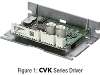
The original CVK series of drivers (hereinafter “CVD”) can produce higher torque, lower vibration, and lower noise compared to conventional stepper motor drivers, but they were not designed to be mounted onto boards. (See Figure 1.)
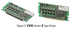
The CVK series S type driver (hereinafter “CVD-S”) was developed to be mounted onto self-built control boards, while maintaining the same characteristics as the CVD series. (See Figure 2.)
This article discusses the functions and specifi cations that were newly added when developing the CVD-S series while considering that it would be mounted on self-built control boards, as well as the technical background to the development.
2. Features
2.1. Overview
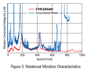
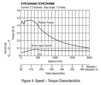
CVD drivers achieve less vibration, less noise, higher stop position accuracy, and higher torque characteristics than conventional models. (See Figures 3 and 4.)
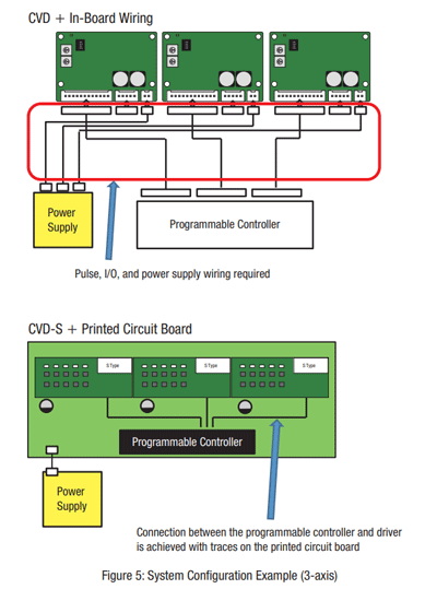
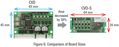
CVD-S drivers have the same characteristics as CVD drivers, but are smaller and have more functionality. They are smaller than CVD drivers since they don’t contain an I/O photocoupler, electrolytic capacitor, or switches. The connector has also been turned into a pin header, thus saving more space and increasing I/O functionality. (See Figures 5 and 6.)
2.2. Product Line
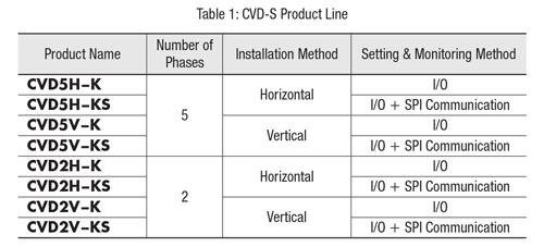
The CVD-S series has a product line of 8 types of drivers, with different numbers of phases, installation methods, and setting methods. (See Table 1.)
Although each of them carries out operation commands with pulses, either I/O (I/O setting type) or I/O + SPI communication (SPI communication setting type) can be selected for the setting and monitoring method.
With the CVD series, drivers that were optimally adjusted for each motor rating were necessary, but with the CVD-S series, either I/O or SPI communication can be selected so that the optimal settings for each rated motor can be used with a single driver (0.35 to 2.8 A/phase).
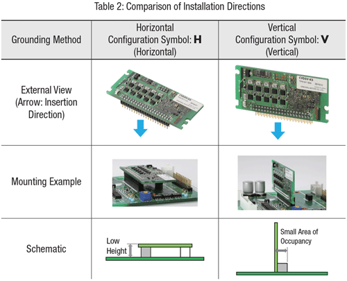
The CVD-S series offers two installation directions, depending on the method of installation. The customer can select whether they want to reduce the height or the area of occupancy according to their equipment. (See Table 2.)
2.3. Circuit Configuration
The main changes in the CVD-S series from the CVD series are as follows.
1) Separation of Control Power Supply and Main Power Supply
The control power supply (5 VDC) and the main power supply (24 VDC) have been separated so that monitoring and settings can still be made with SPI communication when the main power supply is disconnected.
2) External Installation of Electrolytic Capacitor
The CVD-S series does not have an electrolytic capacitor for a power supply. This means that a power supply electrolytic capacitor can be freely arranged on the customer’s control board. (Recommendation: Capacity 680 μF, withstand voltage 50 VDC.)
3) I/O Input of Function Switches
Functions that were set with switches in CVD drivers can now be set with either I/O or SPI communication.
4) Changes to I/O Specifi cations and Additional Points
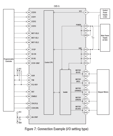
CVD-S drivers are directly mounted on the customer's board. This means that the I/O component does not need to be insulated, and there is no longer a photocoupler due to CMOS input and open collector output.
The connector has also been turned into a pin header, thus saving more space. Since this allows for more pins in a small space, functions set with switches can be input with I/O, and more functions can be added. A connection example is shown in Figure 7.
3. Heat Measures
3.1. Overview
Heat measures are a major issue for motor drivers. If a lot of heat is generated, the mounting position must be adjusted, a heat sink must be installed, forced cooling is required, and so on. Since there is not much room for heat measures in small devices, any changes made to self-built control boards involve tremendous effort.
Like the CVD series, the CVD-S series offers lower heat generation and increases heat dissipation through the use of a low-loss switching element.
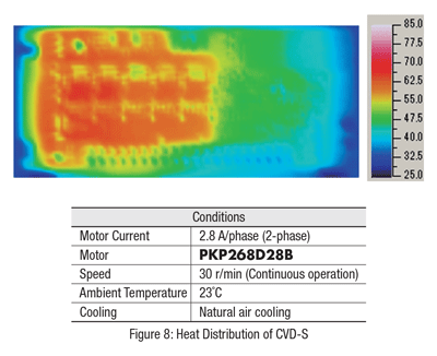
Figure 8 shows the driver's heat distribution during operation (thermographic image). Measurements were made at low-speed operation under extreme driver heat conditions, with a maximum current setting of 2.8 A/phase. Under these measurement conditions, it operated within normal range even with just natural air cooling, with no alarms generated, up to a maximum of 68 ˚C (ambient temperature+45 ˚C).
3.2. Use of a Low-Loss Switching Element
The switching element that controls motor current (Nch MOSFET; hereinafter “FET”) is one of the electronic parts in a driver that generates a lot of heat. The main cause of FET heat generation is conduction loss, which increases in proportion to the degree of ON-resistance when current flows to the element. The CVD-S series uses a low-loss FET that decreases the ON-resistance of the FET in conventional products to 1/20 the amount, similar to the CVD series. This reduces the amount of heat generation itself.
3.3. Pattern Design that Takes Heat Dissipation to the Printed Circuit Board into Consideration
It is important to keep the temperature of the FET low in order to ensure its reliability. Previous driver heat measures before the CVD series were to suppress temperature rise to the specifi ed value by dissipating heat generated by the FET to an external aluminum heat sink. In contrast, the CVD and CVD-S series offer a printed circuit board that itself effectively functions as a heat sink, thus eliminating the need for an external aluminum heat sink. This means that the heat resistance of the printed circuit board must be lowered, and the following designs were made with this in mind.
1) As Much Copper Foil Area as Possible
2) Parallel Connection of Through-Holes
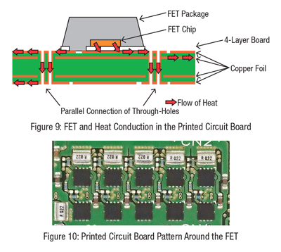
The FET also employs a device with a package that efficiently transmits heat generated inside the element to the printed circuit board. Figure 9 shows a cross-section schematic of a CVD-S printed circuit board, and Figure 10 shows an actual printed circuit board pattern.
Heat generated by the FET is dissipated by transmitting it to the copper foil on the printed circuit board.
By lowering the amount of heat generated and designing a heat dissipation structure in the printed circuit board, the output current can be increased without installing an external aluminum heat sink.
4. I/O Functions of CVD-S
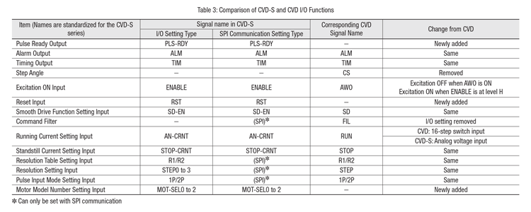
The CVD-S series offers both an I/O setting type and SPI communication setting type. The changes in the I/O functions from the CVD series are shown in Table 3.
By adding a reset input and a motor model number setting, the circuit is simplifi ed, the customer needs fewer self-built control boards, and fewer models are needed as well.
1) Pulse Ready Output (PLS-RDY)
This is an output signal that notifi es the user that the device is operational.
When all of the following conditions are met, PLS-RDY switches to level L.
· The control power supply and main power supply are input.
· No alarm has been generated.
· RST is level H.
· An excitation command is being input.
· The internal state is operational (SPI communication setting type).
2) Resolution Settings (R1/R2, STEP0 to 3)
A total of 32 settings are possible with a combination of five input signals. The values that can be set are the same as in the CVD series.
They can be set via SPI communication in the SPI communication setting type.
3) Motor Model Number Setting Input (MOT-SEL0 to 2)
In the CVD series, high performance is achieved by setting optimal parameters for each motor.
In the CVD-S series, three input signals are used to select from six settings according to the rated current of the motor being used.
Since optimal settings can be used with a single driver for each rated motor, this reduces the number of CVD-S drivers the customer needs.
Motor changes can be adapted to, even if the CVD-S driver has been soldered. Therefore, even if the same self-built control board is being used in equipment with different motors, the CVD-S driver can be installed beforehand. This means that fewer self-built control boards are needed, and fewer models are needed as well.
4) Running Current Setting Input (AN-CRNT)
The running current can be set with analog voltage. Since the value is analog, it can be set more fi nely than in the CVD series.
The running current can also be set according to the load conditions and operating pattern in order to suppress heat generation.
5) Reset Input (RST)
Resolution and motor model number settings are reflected either when the control power supply is reset or RST is used, rather than being reflected in real time.
Since the settings can be refl ected without resetting the entire control power supply of the self-built control board, this simplifi es the power supply circuit.
5. CVD-S SPI Communication Function
5.1. Overview
In CVD-S drivers (SPI communication setting type), various parameters can be set and status monitoring is possible via SPI communication.
Using SPI communication not only decreases the number of connection terminals on the self-built control board, but also allows for more settings and monitoring than with I/O. This increases the functionality and ease of maintenance of the customer’s equipment.
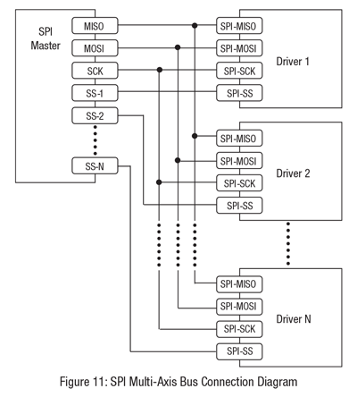
SPI communication is a clock synchronization point-to multipoint serial communication method that is widely used in on-board communication between ICs. (See Figure 11.)
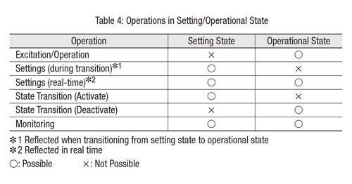
In the CVD-S series (SPI communication setting type), a unique communication protocol is used. Besides settings and monitoring commands, there are also state transition orders. The details that can be communicated differ for each state. (See Table 4.)
When an ACTIVATE command is issued, the driver transitions from the setting state to the operational state, and when a DEACTIVATE command is issued, the driver transitions from the operational state to the setting state.
The settings reflection timing differs depending on whether the set parameters are for real time or when ACTIVATED.
5.2. Items that Can be Set
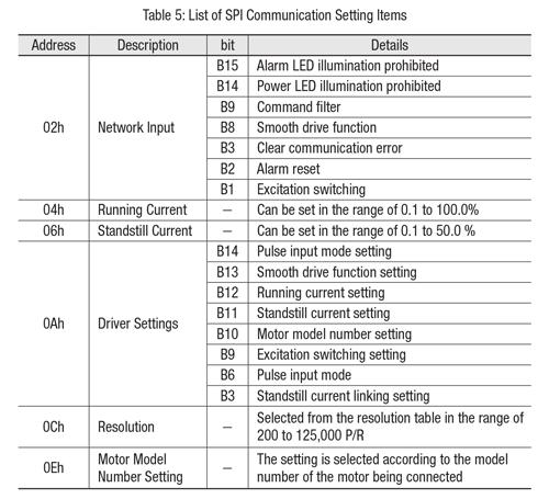
The items that can be set with SPI communication are shown in Table 5.
The items that can be set with the I/O setting type can all be set with SPI communication as well.
Some functions can also be set from I/O, rather than SPI communication. Whether a function is set via either SPI communication or I/O can be set using SPI communication. (Examples: Smooth drive function setting, running current setting)
Unlike the I/O setting type, the SPI communication type allows running current and standstill current to be set individually (standstill current linking setting). This makes heat measures easier to carry out through the current settings.
5.3. Items that Can be Monitored
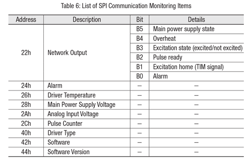
The typical items that can be monitored with SPI communication are shown in Table 6.
· Overheat
The overheat bit outputs when the temperature is lower than the temperature at which an overheat alarm is generated.
Since the motor switches to a non-excited state and stops when an overheat alarm is generated, the overheat bit is a measure for lowering the temperature before that happens.
· Pulse counter
The number of pulses recognized by the driver can be obtained. This can be used to check for malfunctions due to noise and as a debugger during development by comparing with the number of pulses from the programmable controller.
· Alarm code
The cause of the alarm can be determined at the host level without checking the number of LED blinks, making it easier to respond to problems.
6. Conclusion
CVD-S drivers were developed for customers who use stepper motors with self-built control boards. Without losing the low-vibration, low-noise, and high-torque characteristics of the CVD series, it can be mounted onto printed circuit boards, contributing to both smaller and higher performance equipment. By using a switching element with little loss as a measure against heat, which is an issue with mounted drivers, and employing a heat dissipation structure in the printed circuit board, heat generation is drastically reduced. The CVD-S series also has additional I/O functions and SPI communication functions.Oriental Motor will continue to expand on the new technologies that were generated with the development of the CVD-S series, and continue to develop products that meet our customers’ demands.
